CN
  • Home
  • Product
    Conductive silicon carbide substrate Optical SiC Wafer
  • Research strength
    Scientific Research Strength Patent Achievements
  • News
  • About us
    Company Profile Corporate Culture Social Responsibility
  • Join us
  • JSG
  • Home
  • Product
    Conductive silicon carbide substrate Optical SiC Wafer
  • Research strength
    Scientific Research Qualification Patent Achievements
  • News
  • About us
    Company Profile Enterprise Dynamics Social Responsibility
  • Join us
  • JSG
  • CN
PRODUCTS
Conductive silicon carbide substrate Optical SiC Wafer
  • SuperSiC
    Conductive silicon carbide substrate
    Third generation semiconductor materials
    Master the industry-leading 6-12inch silicon carbide crystal growing technology,and hold independent and controllable large-size silicon carbide crystal growing and processing technology.
    View more
  • SuperSiC
    Optical SiC Wafer
    Third generation semiconductor materials
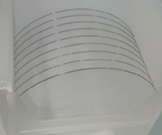
    SuperSiC possesses industry-leading 8–12 inch optical-grade silicon carbide crystal growth technology, featuring self-controllable capabilities for the growth and fabrication of large-size optical-grade SiC crystals.
    View more
SuperSiC
ABOUT SUPERSIC Company Profile Enterprise Dynamics Social Responsibility Join Us
FOLLOW US
SuperSiC
Facebook
SuperSiC
Linkedin
SuperSiC
Twitter
SuperSiC
Wechat
NO 009 Shunyuan Road ,East Second District Shangyu Economic and Technological Development zoon ,Hangzhou Bay,Shaoxing City,Zhejiang Province, China
Email:supersic@jsjd.cc Phone:0575-82723280(分机号5888)
@2023 superSIC All Rights Reserved. 浙ICP备2023007127号-5浙公网安备33060402001863号
东方四通
Website Map
Powered by : HANSUN